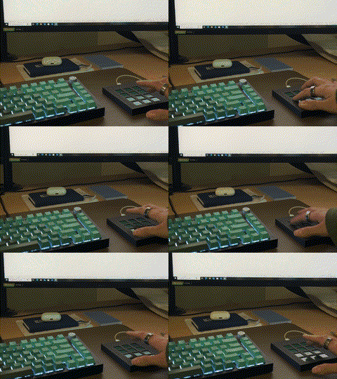
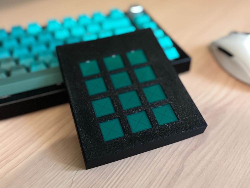
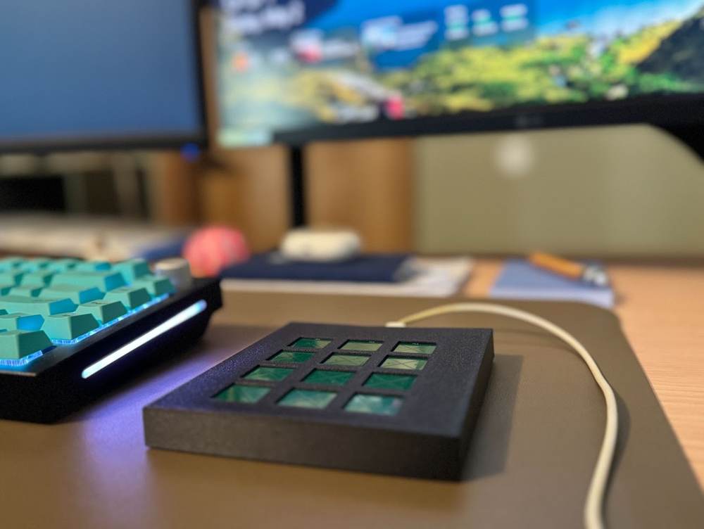
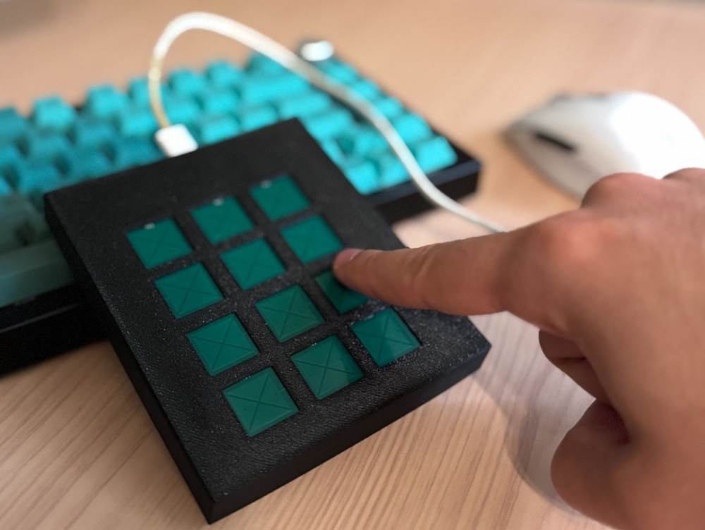
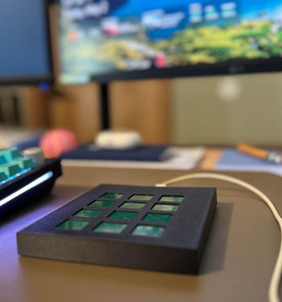
Capacitive and haptic electronics have been an idea companies have flirted with for years. You’ll find capacitive numpads living inside calculators, smartphones, door keypads, and even modern laptops. But when it comes to consumer PC keyboards, capacitive tech is still not in the mainstream. Why? Because flat, silent keys with no physical response just don’t cut it for users who love that tactile click.
STM32
Capacitive Touch
Haptics
PCB Layout
01
Introduction
Capacitive and haptic electronics have been an idea companies have flirted with for years. You’ll find capacitive numpads living inside calculators, smartphones, door keypads, and even modern laptops. But when it comes to consumer PC keyboards, capacitive tech is still not in the mainstream. Why? Because flat, silent keys with no physical response just don’t cut it for users who love that tactile click.
Apple gives you a sleek glass surface with the Magic Trackpad. Asus tried blending a numpad into a touch surface. But neither solves the real issue: how do you keep the clean aesthetic of capacitive interfaces without losing the satisfying feedback of mechanical keys?
That’s the challenge I set out to solve — and the result is my capacitive-haptic keyboard: a fusion of slim, modern input design and punchy, haptic feedback that feels great to type on. It’s not just a concept; it’s a step toward keyboards that look futuristic but feel familiar.
02
Project Overview
I had an absolute blast building this project — it brought together the best parts of hardware design, embedded software, and 3D design. Even better, it’s not just a fun prototype — it’s now my daily driver! In this project, I wanted to create a functional and expandable capacitive-haptic keyboard. Key areas of focus included:
Custom Capacitive Touch Design: Rather than relying on off-the-shelf buttons, I wanted the board to have capacitive sensing buttons. More so, I wanted the buttons directly in the PCB's layout, staying true to the keyboard's low-profile requirement.
Custom Capacitive Touch Design: Rather than relying on off-the-shelf buttons, I wanted the board to have capacitive sensing buttons. More so, I wanted the buttons directly in the PCB's layout, staying true to the keyboard's low-profile requirement.
Haptic Feedback Integration: Capacitive buttons alone don't feel good. The product, using both SW and HW, should deliver responsive, per-key tactile feedback, ensuring tight integration between touch detection and haptic actuation.
Haptic Feedback Integration: Capacitive buttons alone don't feel good. The product, using both SW and HW, should deliver responsive, per-key tactile feedback, ensuring tight integration between touch detection and haptic actuation.
Sleek Design: I wanted to create a design that matched my current keyboard while also staying true to the sleek and aesthetic profile.
Sleek Design: I wanted to create a design that matched my current keyboard while also staying true to the sleek and aesthetic profile.
03
Picking Components
04
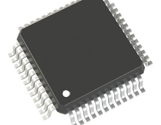
STM32F072CBT6
I picked this ST microcontroller for 2 major reasons.
1) It has ST's Touch Sense Controller (TSC) hardware. This will allow our capacitive sensing to be done without complicated math.
2) Since we are making a keyboard, USB will be needed. This MCU allows us to use USB 2.0 without any additional hardware (like crystals or even in-line resistors).
05
USB-C
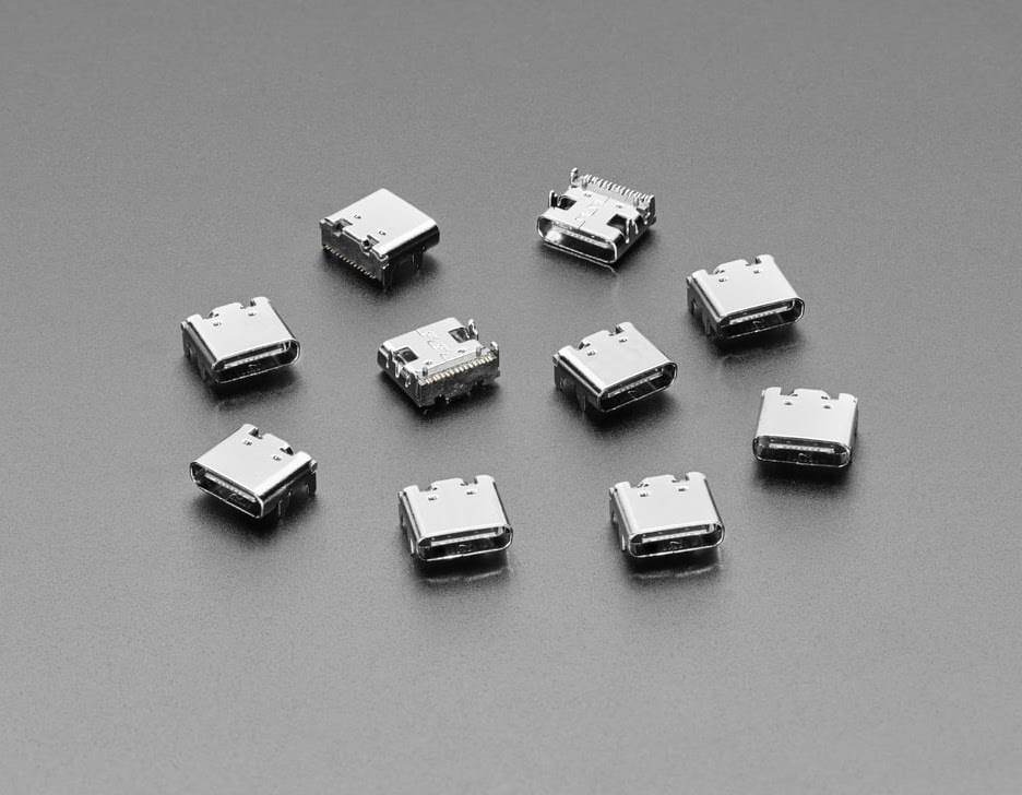
USB-C is common in most products now, so I wanted the keyboard to be relevant. This would also be great for a keyboard that is constantly being plugged/unplugged. We can get data transfer, power, and easy connecting.
06
DRV2605LDGSR
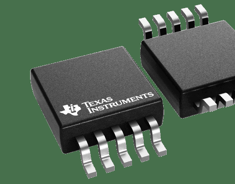
Haptics! This IC is the brain of the haptics in the keyboard. It is neat in that we can control vibration motors with built-in effects with nothing but I2C.
07
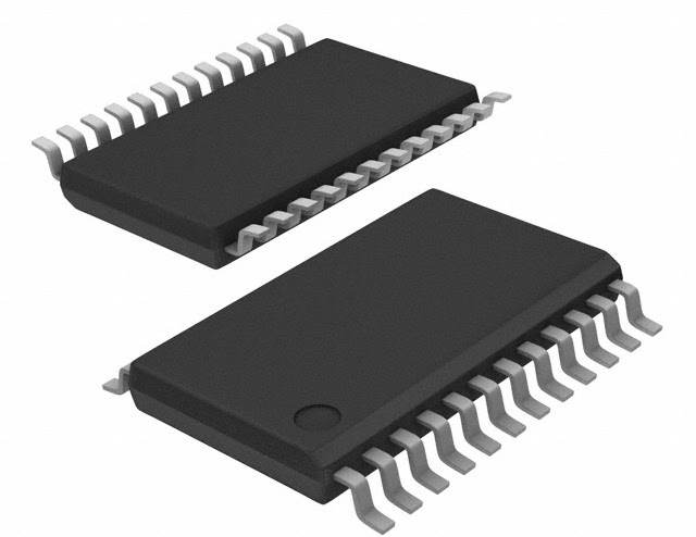
PCA9548APWR
As nice as the DVR motor controller is, it only has 1 non-configurable address. I didn't want to overcomplicate the circuit so we can throw in some I2C muxes to talk to a multitude of DVR controllers for a per-key haptic effect.
08
DC Vibrating Motors
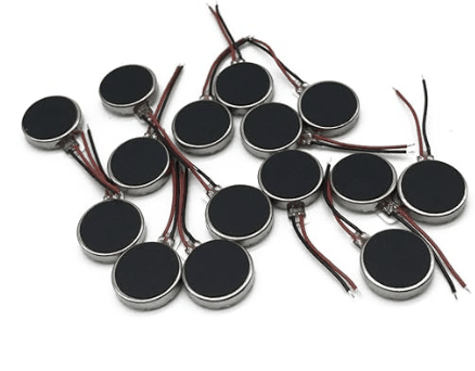
I didn't spend too much time looking into the type of motor I wanted for this project. The main requirement was that they would be able to be driven by our circuit voltage. The DRV is great in that it compensates for all kinds of motors (including cheap Amazon ones)
09
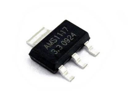
AMS1117
This neat little component is a simple LDO to get us from our PCs' 5V power (from USB) to 3.3V, the voltage all of our components require to properly work.
10
Creating the Schematic
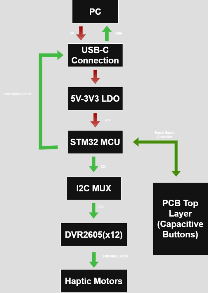
How do we put all the components together? A block diagram can help us picture how the system will function. Remember, when the user taps on a capacitive key, we want feedback from our vibration motor AND the relevant numpad press sent to the computer. For the best kind of feedback, we will need a motor under each key. This means we will have to distribute the signal press to any of the 12 numpad keys. Now we can draw a simplified block diagram to help us lay out our schematic.
This post focuses on the new and interesting design aspects of this project. Standard components—like the ST-Link programming interface, LDO selection, and ST’s MCU best hardware design practices—are reused from earlier designs and won’t be covered here.
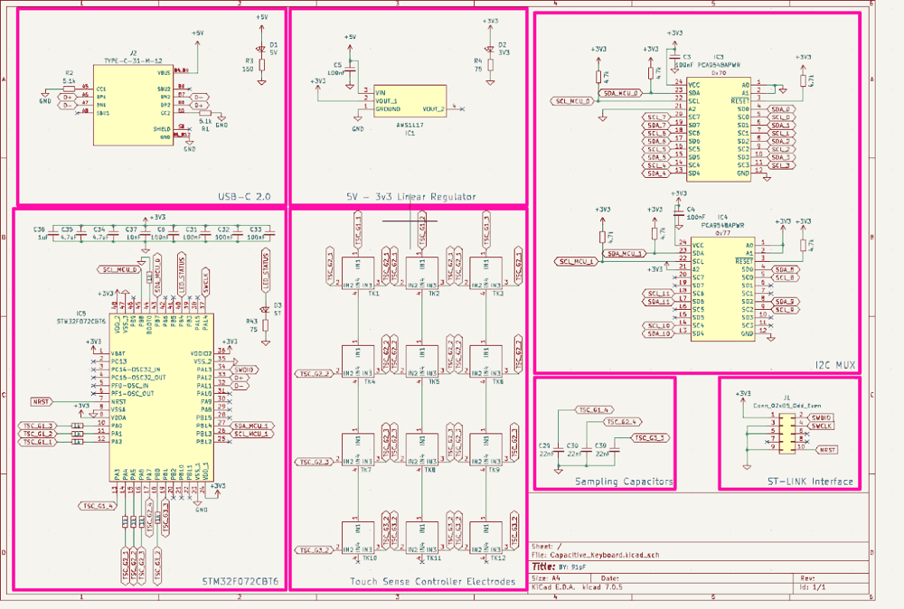
STM Touch Sense Controller: In terms of the button's design, we will be covering more about the background of the TSC and how it works when we design the PCB. For the schematic, we only need to follow a few guidelines.
1) To save on pins, we can implement a matrix configuration (3 rows × 4 columns) to scan 12 capacitive keys using only 7 TSC IOs, instead of 12 dedicated lines. This significantly reduces pin usage. Since STM32’s TSC groups each set of 4 IOs under a common sampling capacitor, our 7 IOs span 3 groups—requiring 3 external sampling capacitors. This brings our total TSC pin requirement to 10 (7 for sensing, 3 for sampling). Had we not used a matrix configuration, we would have needed a minimum of 12 pins simply to account for the 12 buttons.
2) Another thing to note about ST's TSC is that it does not allow mutual capacitance sensing. So, each key in our design is split into two capacitive pads—one tied to a row, the other to a column—allowing us to detect their intersection. This works with STM32’s TSC, which doesn’t support mutual capacitance. This will be made more clear when we create our custom keypad footprints. All you have to know now is that we will NOT be using mutual capacitance.
3) Along with the sampling capacitor per grouping, each TSC driving pin requires a series resistor. This resistor is used to help an RC time constant that the TSC uses to sense capacitance changes. The documentation recommends anywhere from 470 ohms to 10k ohms. Choosing a resistor that’s too small results in fast charge times and reduced sensitivity, while values that are too large risk missing touch events due to slow response. Based on the matrix’s physical span (~3 inches), we opted for 1 kΩ as a balanced choice for sensitivity and response time.
This same thought process was used for the sampling capacitor. ST recommends anywhere from 10nF to 100 nF, where our capacitance would change sensitivity or response time. In this case, 22nF seems like a good compromise. While ST recommends experimenting with various resistor and capacitor values to tune performance, doing so requires multiple PCB revisions or a robust dev board. To avoid this, we selected midrange values (1 kΩ and 22 nF) that provide a good baseline and can be adjusted for in firmware.
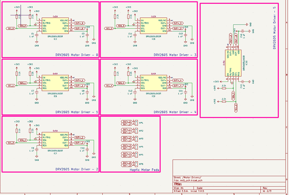
Motor Control: The approach taken for motor control was not the cheapest approach. Each DRV2605 haptic driver costs approximately $1.80, and due to its fixed I²C address, we need two I²C multiplexers (~$3 each) to control all 12 motors independently. While we considered multiplexing a single DRV2605 to reduce cost, TI strongly advises against this. The driver’s differential output is tuned to a specific motor’s characteristics, and switching loads introduces impedance mismatches and calibration issues, likely to yield poor or inconsistent haptic feedback.
The 12 DVR2605 and mux approach also offered more simplicity in the design. All that was needed were 2 I2C peripherals from the MCU, pull-up resistors for the muxes, and then the DVR2605 (with their pull-up resistors). Using dedicated drivers and I²C muxes simplifies firmware and signal integrity: the MCU enables one mux channel at a time and communicates with the desired DRV2605 via I²C, ensuring clean, consistent motor control.
11
Creating the PCB
Understanding TSC
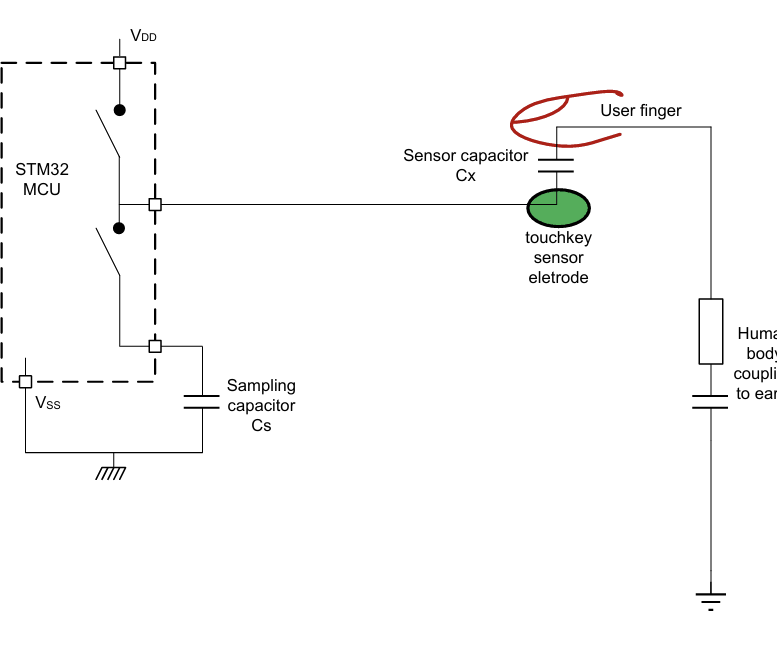
Before going into the layout and design of the capacitive buttons, I want to touch a bit more on how ST's TSC works. The basis of it is simple. When a human (the user) touches a capacitive button, the overall capacitance increases. When your finger (a conductor) approaches the sensor (another conductor), we get a parallel capacitor with the pad. So how does the TSC use this to know when it is being pressed? This is where the sampling capacitor we mentioned earlier comes into play.
The pad sensor (Cx) is charged to a specific voltage (VDD) by the TSC. That accumulated charge is then transferred into the sampling capacitor (Cs). The pad sensor continues to be charged, and the charge is transferred until the sampling capacitor reaches a specific voltage threshold. You can then count how many charge transfers it took to get Cs to reach that threshold. Now, if we touch Cx (the pad sensor), then we know the capacitance increases. Each charge and transfer 'fills' the sampling capacitor faster. This change in the amount of charge transfers lets the TSC know that we have touched the pad.
Creating the Pad
So we understand how this will all be connected and how the TSC works. Now how do we actually design this? We wanted to integrate this into our PCB, so the first step is designing the 'button' footprint. There are a few guidelines ST says to follow when creating the button:
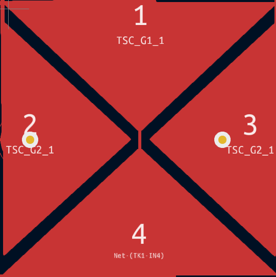
1) Make the button the size of the intended touching object. Since a finger was the intended use for this, I made the size of the pad the size of an average human's finger.
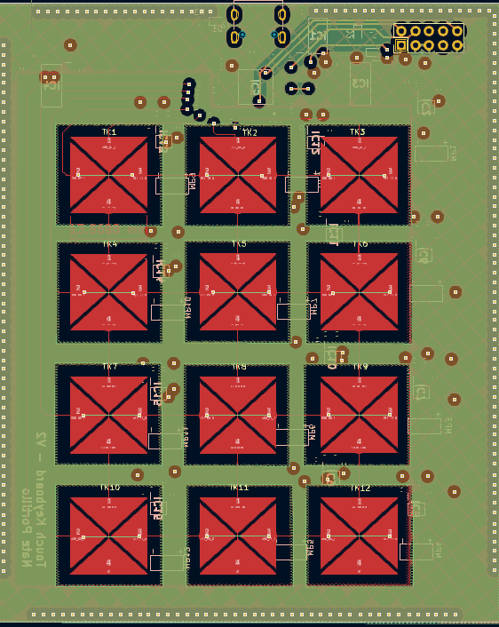
2) Since mutual capacitance isn't supported, each button should essentially be two buttons that form one. If you look closely at the button, column 1 would drive pads 1 and 4 while row 1 would drive pads 2 and 3 (connected with the vias).
Creating the Matrix
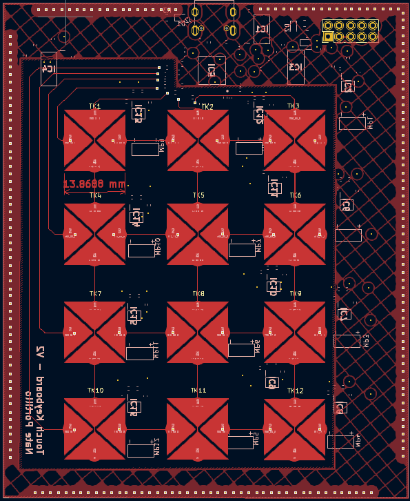
Now that the pad has been created, the matrix can be formed. Best practice is to keep all components away from the pads, as we do not want to affect the capacitance or introduce noise in any way. Additionally, we route the TSC driving lines (the traces) as short and as far away from the buttons' touch zone as possible. We have a total of 7 driving lines that interconnect the pads to form the matrix so any pad touched will transfer the charge for 2 TSC lines. Lastly, a hatched GND plane is added to help isolate the pads from any noise.
Creating the board layout
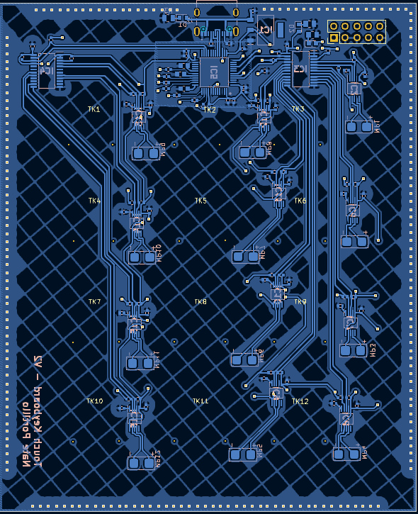
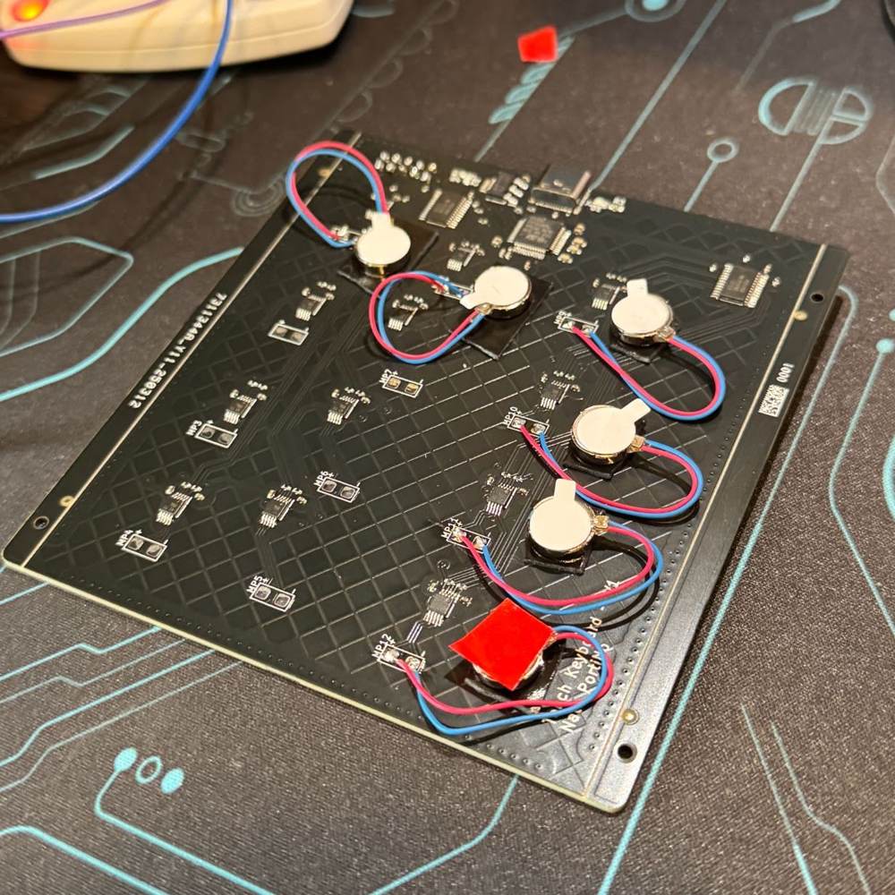
To optimize touch sensor performance, all components were placed on the bottom side of the PCB and routed carefully to avoid running traces directly beneath any of the touch pads. This minimizes interference and stray capacitance. A hatched GND plane was used underneath the touch area instead of a solid plane. This is because a solid GND plane can create excessive parasitic capacitance, potentially overwhelming the signal caused by a finger touch. The hatched pattern provides EMI shielding and a stable ground reference while keeping the baseline capacitance low enough for reliable sensing.
Creating the stackup
JLCPCB was offering a deal on 4-layer boards, so I took advantage of it to simplify routing. I chose the following layer stackup: Top Layer (Touch Sensors) – GND Plane (with sensor pad routing) – 3.3V Power Plane – Bottom Layer (Signal Routing).
Having dedicated power and ground planes significantly reduced the need to manually route those signals. Routing the sensor pad connections within the GND layer also allowed me to avoid passing sensitive touch signals near noisy components or digital traces, which could otherwise affect sensing performance.
A critical design detail was maintaining keepout zones under the capacitive touch pads. Placing solid copper directly beneath the sensors would increase parasitic capacitance and reduce sensitivity, so those regions were left free of copper. This is visible in the layout as open areas (green or orange, depending on the layer view) beneath the touch pads.
12
Arrived Boards - Issues, Testing, and Assembly
V1 Mistake
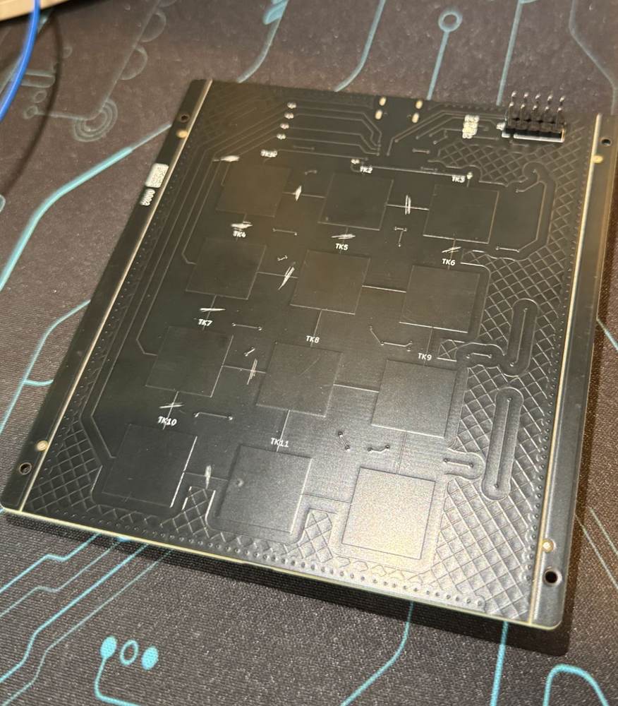
While the earlier sections might make it seem like everything went smoothly, Version 1 of the board had a critical design flaw that I initially overlooked. The intention was to use a matrix configuration, where each key is formed by the intersection of a row and a column pad, each connected to separate TSC lines. However, instead of splitting each key into two electrically isolated pads (one for the row, one for the column), I mistakenly connected both TSC lines to a single, continuous copper pad.
Visually, it looked like a proper matrix layout — rows and columns were routed correctly — but electrically, the entire sensor grid behaved like one giant touch pad. As a result, touching any key affected all of them, and individual key detection was impossible.
The issue is hardware is NOT cheap. So, I took an X-Acto knife and cut the traces to electrically isolate 7 pads (the ones directly connected to the TSC lines). This will allow me to create the firmware and test the haptic feedback functionality before correcting the issue and spinning up a new board.
13
Testing on V1
Using V1, I was able to write quick and dirty code to make sure that the sampling capacitor and resistor sizes were fine, the muxes were able to communicate, and the drivers were working properly with my selected motors.
14
Building V2
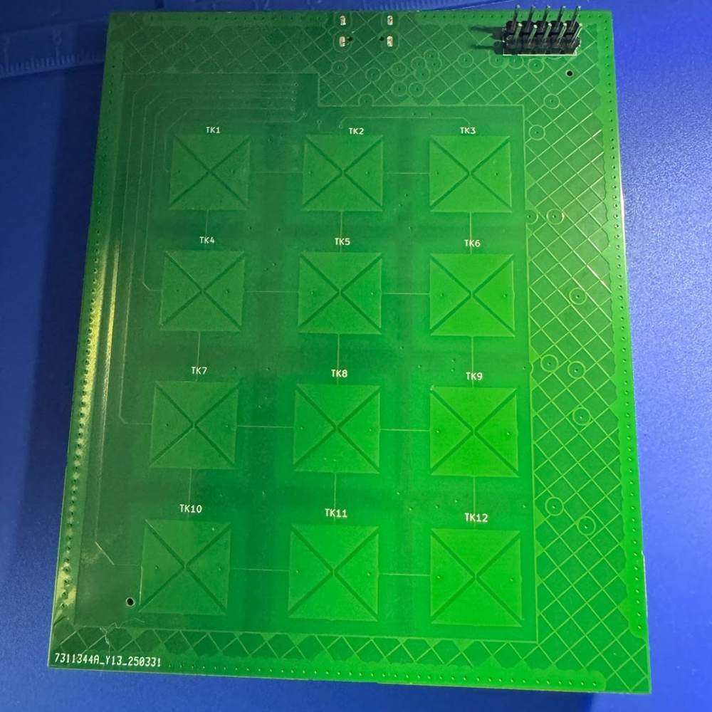
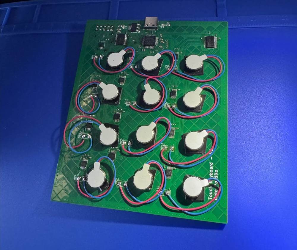
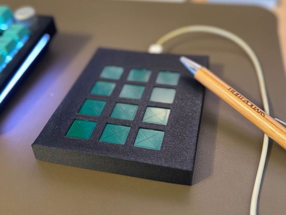
Once core functionality was confirmed on V1, I spun V2 up with the pad design I showed earlier in the blog. Unfortunately these had to be green, as black was too expensive a second time around.
15
Assembling V2
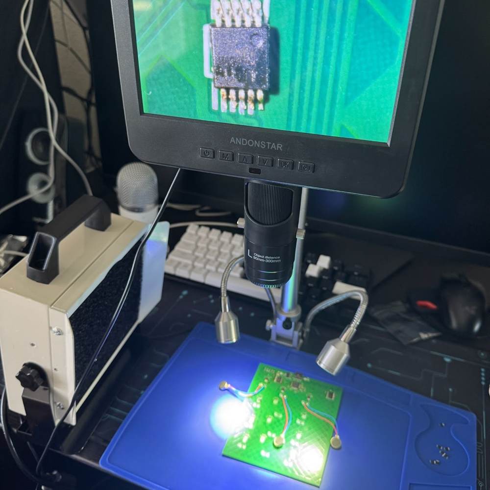
Remember when I mentioned components were expensive? This mean I did not want to order another batch. So I ordered V2 as unassembled boards, desoldered all the components from V1, and resoldered them myself on the V2 board. This was an extremely fun but tedious process.
After a few days of soldering, I had completed the boards (and saved a ton of money)! This means we can officially create and complete the firmware for the board.
16
Programming the Microcontroller
17
Pinout Configuration
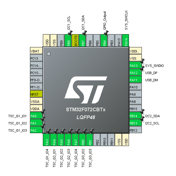
Based on our requirements we set up a few peripherals:
1) USB (DP & DM for data transfer)
2) SWDIO & SWCLK (For programming)
3) I2C (x2, for our 2 muxes)
4) TSC (3 groups with 1 sampling capacitor per group)
18
Setting up TSC
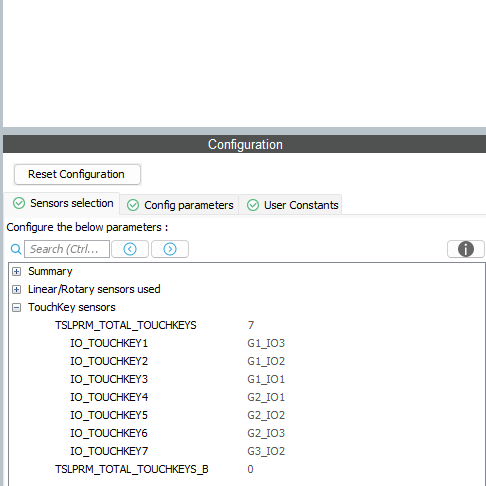
Before tuning the TSC, we first needed to define the type and layout of the touch sensors in the middleware. This step involves assigning each touch key according to its corresponding row and column, so the firmware can drive and detect them correctly.
As mentioned earlier, we're using a matrix configuration that allows us to scan 12 keys using only 7 TSC pins—3 rows and 4 columns—greatly reducing GPIO usage.
19
Setting up TSC
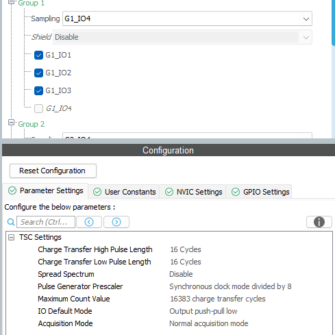
After some trial and error, the Touch Sensing Controller (TSC) was configured to achieve the desired sensitivity across all keypads.
Charge transfer pulses: These define how long the GPIO stays high and low during each transfer cycle. Increasing the high pulse duration improved sensitivity—especially for keys with longer traces, which were initially too weak to detect reliably. The low pulse duration was also adjusted accordingly to maintain timing balance.
Charge transfer pulses: These define how long the GPIO stays high and low during each transfer cycle. Increasing the high pulse duration improved sensitivity—especially for keys with longer traces, which were initially too weak to detect reliably. The low pulse duration was also adjusted accordingly to maintain timing balance.
Maximum count value: This sets the upper limit on how many transfer cycles the TSC will attempt before timing out. A higher value increases sensitivity by allowing more time for the sampling capacitor to accumulate charge, but it comes at the cost of slower scanning speed.
Maximum count value: This sets the upper limit on how many transfer cycles the TSC will attempt before timing out. A higher value increases sensitivity by allowing more time for the sampling capacitor to accumulate charge, but it comes at the cost of slower scanning speed.
These values could likely be optimized further, but they performed well for the intended use case and provided consistent detection across all keys.
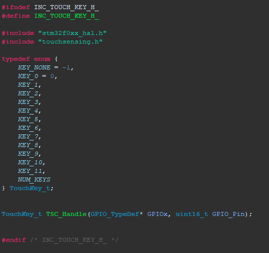
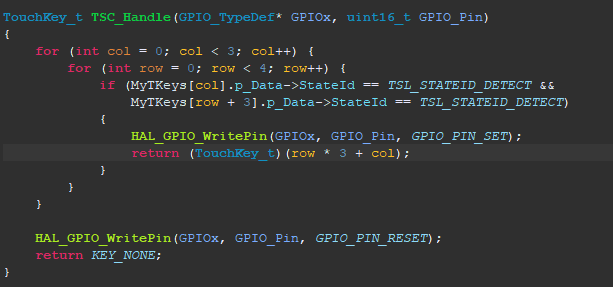
The TSC_Handle() function scans our 3×4 capacitive touch matrix to determine which key is currently being pressed. Each key is formed by the intersection of a row and a column electrode. The touch-sensing middleware updates an array called MyTKeys[], where each entry contains a state such as TSL_STATEID_DETECT (indicating a touch).
The function loops through all possible row-column combinations, and when it finds a simultaneous touch on a row and a column, it calculates the key index using (row * 3 + col). This gives us a unique index from 0 to 11 and returns the corresponding value from the TouchKey_t enum (KEY_0 to KEY_11). If no key is detected, the function returns KEY_NONE.
The enum makes the code easier to read and manage by giving each key a descriptive name instead of using raw integers. A GPIO pin is also toggled high when a valid key is pressed—this was particularly useful for debugging without having to transfer values over USB.
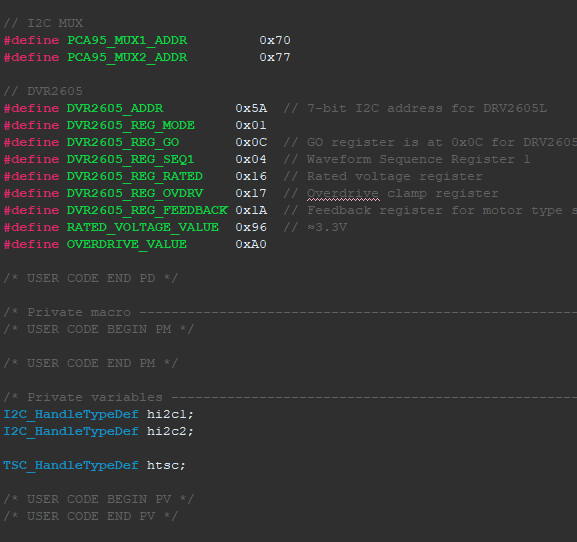
To manage the DRV2605 haptic motor drivers, a set of macros was defined. The first two macros define the addresses of the I²C multiplexers, which are needed because all DRV2605 devices share the same fixed I²C address. This setup allows each motor to be isolated and accessed through a unique channel on a mux.
The additional macros define the DRV2605’s internal registers This includes setting the operation mode, trigger control, waveform sequence, rated voltage, overdrive voltage, and feedback configuration.
Operation Mode
This sets the driver to operate in "internal trigger" mode. In this mode, once the waveform is loaded and the GO command is sent, the DRV2605 will automatically play the haptic effect without needing continuous control.
Rated Voltage
This sets the normal operating voltage for the motor. It affects how much power is delivered during a typical effect. A voltage too low may result in weak haptics, while too high could stress the motor. This value was selected based on the system's 3.3V power supply and the motor’s rated specs.
Overdrive Voltage
This controls the initial kick or intensity of the haptic effect by allowing a brief voltage burst above the rated level.
Feedback Configuration
This tells the DRV2605 whether an ERM or LRA motor is connected and configures internal parameters like braking and drive control.
Waveform Sequence
This register tells the driver which haptic effect to play from its built-in library of effects (such as clicks, buzzes, pulses, etc.).
Trigger Control (GO Register)
Writing to this register tells the DRV2605 to start playing the selected haptic effect.
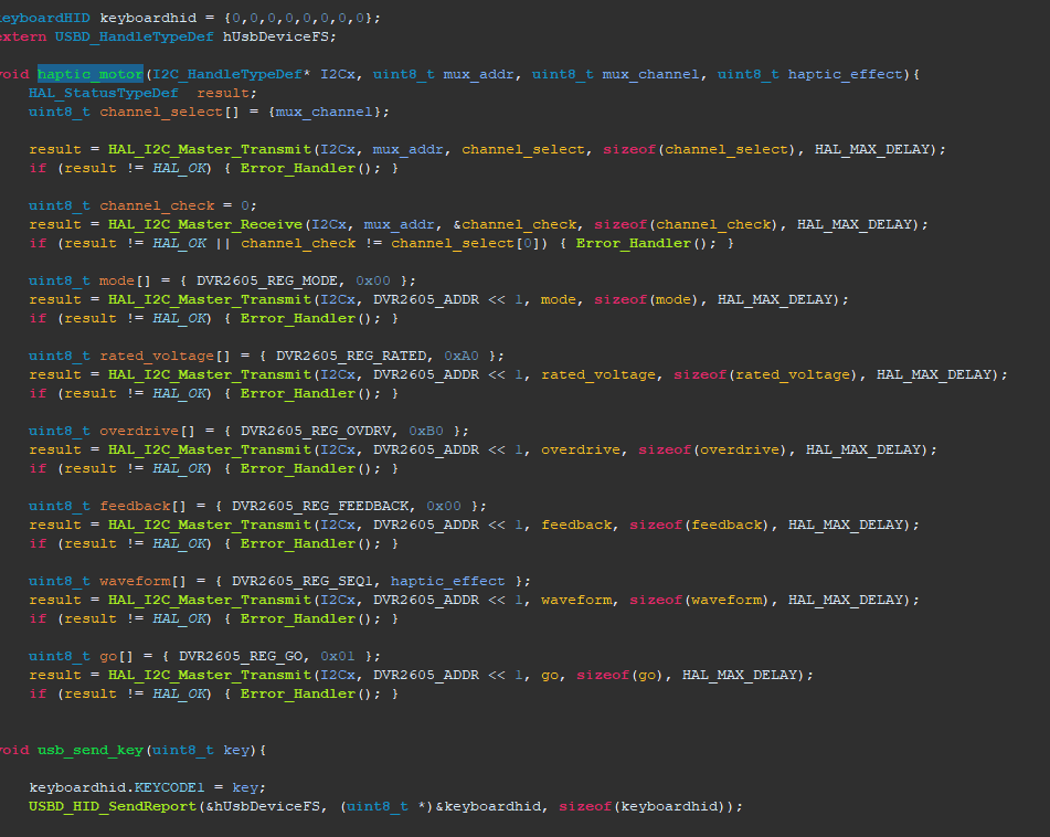
The haptic_motor function handles the full process of activating a haptic effect. It begins by selecting the appropriate mux channel to route communication to a specific DRV2605. The mux is fairly straight; you just need to send an I2C command with the channel you want to be active. Then, it configures the driver by writing to the necessary registers, loads the desired haptic effect, and finally triggers the motor.
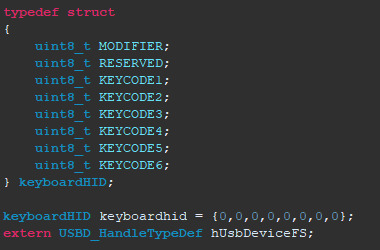
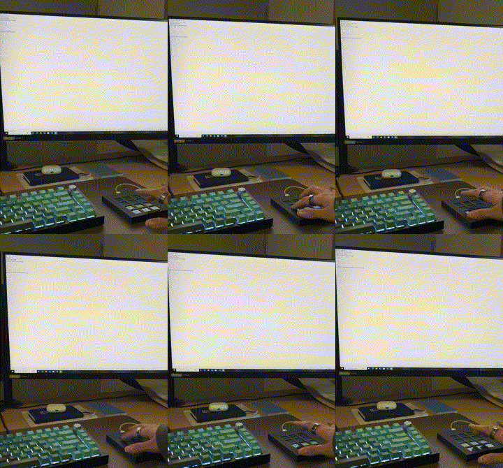
The firmware uses USB HID (Human Interface Device) to send keystrokes to a host computer when a capacitive key is pressed. A custom keyboard HID struct is defined to match the USB HID keyboard report format, which includes fields like modifier keys and up to six keycodes.
When a key is pressed, the usb_send_key() function populates the first key slot in the structure with the corresponding HID keycode (e.g., 0x1E for the "1" key) and sends the struct over USB using USBD_HID_SendReport(). This makes the STM32 appear as a regular USB keyboard to the host system, meaning you can press your capacitive keys and have them type characters on a computer.
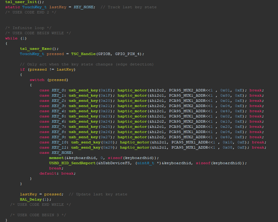
Inside the while loop, the code continuously checks for touch input and responds accordingly.
1) Run TSC sensing: The tsl_user_Exec() function updates the touch state machine and refreshes the status of all keys.
2) Check for key press: The TSC_Handle() function scans the touch matrix to determine which key, if any, is currently being touched.
3) Compare against last key: To prevent repeated keypresses from being sent too often, the code compares the currently pressed key to the last detected one. Only when the key changes does the code take action.
4) Send USB keystroke and haptic feedback: If a valid key is pressed, a USB keystroke is sent and a corresponding haptic effect is triggered using the haptic_motor() function, which selects the correct I²C mux and DRV2605 driver for the touched key.
5) Handle key release: If no key is currently pressed (KEY_NONE), a report with all fields set to zero is sent. This ensures the key release is properly recognized by the host computer.
6) Update the last key: The last key state is updated to the current one so the system is ready for the next touch event.
20
Putting it all together! (Enclosure)
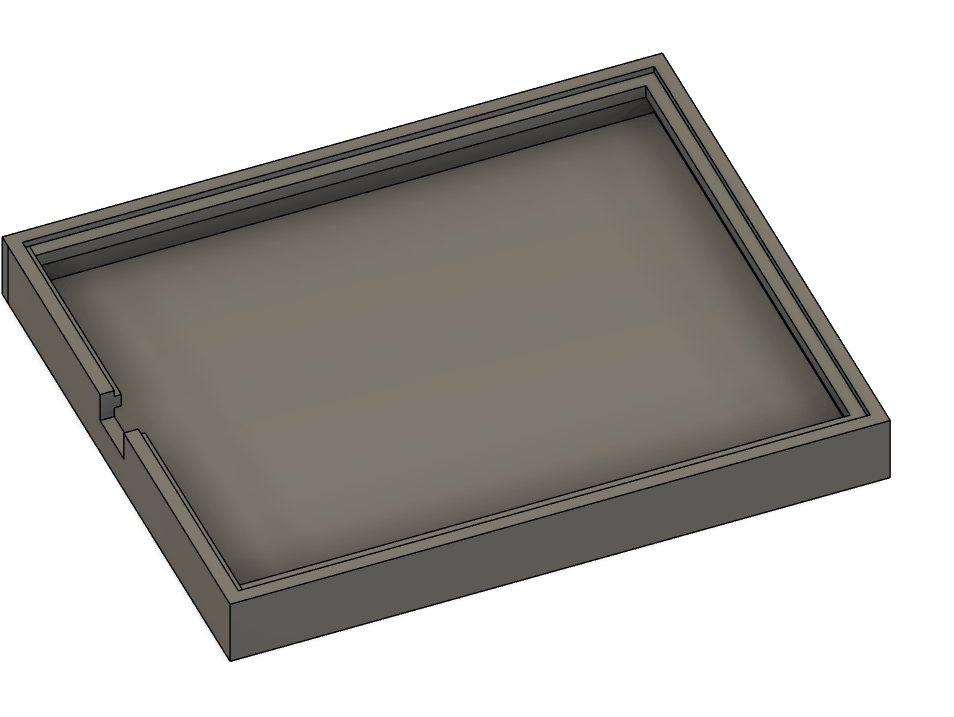
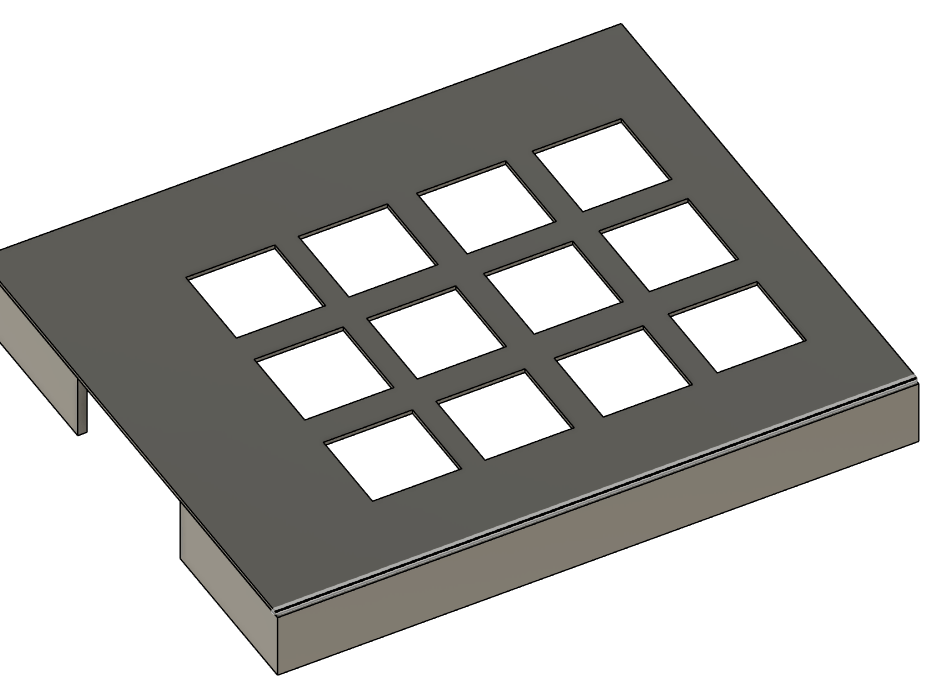
The enclosure (after many iterations) is 3D printed and consisted of a 2-part design. The bottom half holds the PCB and has a hollow center to allow the haptic vibrations to flow through the entire case. Additionally, a top lid with button cutouts keeps the PCB in place and allows for finger presses. I used PETG-CF for maximum durability and a nice carbon fiber texture.
In V3, I would like to re-adjust the TSC parameters to place a nice TPU (flexible material) overlay to hide the PCB and have a softer material for the user to touch.